.JPG)


In this post, we are going to learn a very old grand father of modern processors, named 8085 and his colleague 8255.
Pins, Signals and internal block diagram of 8255:
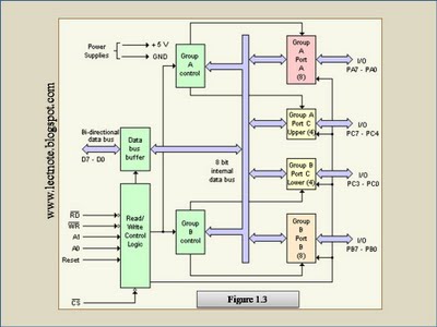
- The internal block diagram of 8255 is shown in fig:
- The 8255 can be either memory mapped or I/O mapped in the system. In the schematic shown in above is I/O mapped in the system.
- Using a 3-to-8 decoder generates the chip select signals for I/O mapped devices.
- The address lines A4, A5 and A6 are decoded to generate eight chip select signals (IOCS-0 to IOCS-7) and in this, the chip select IOCS- 1 is used to select 8255.
- The address line A7 and the control signal IO/M (low) are used as enable for the decoder.
- The address line A0 of 8085 is connected to A0 of 8255 and A1 of 8085 is connected to A1 of 8255 to provide the internal addresses.
- The data lines D0-D7 are connected to D0-D7 of the processor to achieve parallel data transfer.
- The I/O addresses allotted to the internal devices of 8255 are listed in table.
The 8255 has three ports: Port-A, Port-B and Port-C. Port-A can be programmed to work in any one of the three operating modes mode-0, mode-1 and mode-2 as input or output port. Port-B can be programmed to work either in mode-0 or mode-1 as input or output port.
Port-C (8-pins) has different assignments depending on the mode of port-A and port-B. If port-A and B are programmed in mode-0, then the port-C can perform any one of the following functions. As 8-bit parallel port in mode-0 for input or output. As two numbers of 4-bit parallel ports in mode-0 for input or output. The individual pins of port-C can be set or reset for various control applications.
If port-A is programmed in mode- 1/mode-2 and port-B is programmed in mode-1 then some of the pins of port-C are used for handshake signals and the remaining pins can be used as input/ output lines or individually set/reset for control applications. The read/write control logic requires six control signals. These signals are given below:
- RD (low): This control signal enables the read operation. When this signal is low, the microprocessor reads data from a selected I/O port of the 8255A.
- WR (low): This control signal enables the write operation. When this signal goes low, the microprocessor writes into a selected I/O port or the control register.
- RESET: This is an active high signal. It clears the control register and set all ports in the input mode.
- CS (low), A0 and A1: These are device select signals. They are, Interfacing of 8255 with 8085 processor: