Tuesday, 16 August 2011

8255 Programmable Peripheral Interface


         In this post, we are going to learn a very old grand father of modern processors, named 8085 and his colleague 8255.

Pins, Signals and internal block diagram of 8255: 
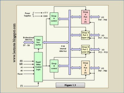


  •  The internal block diagram of 8255 is shown in fig: 
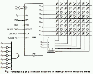
  •  The 8255 can be either memory mapped or I/O mapped in the system. In the schematic shown in above is I/O mapped in the system. 
  •  Using a 3-to-8 decoder generates the chip select signals for I/O mapped devices. 
  • The address lines A4, A5 and A6 are decoded to generate eight chip select signals (IOCS-0 to IOCS-7) and in this, the chip select IOCS- 1 is used to select 8255. 
  • The address line A7 and the control signal IO/M (low) are used as enable for the decoder. 
  • The address line A0 of 8085 is connected to A0 of 8255 and A1 of 8085 is connected to A1 of 8255 to provide the internal addresses. 
  • The data lines D0-D7 are connected to D0-D7 of the processor to achieve parallel data transfer. 
  •  The I/O addresses allotted to the internal devices of 8255 are listed in table. 
              It has 40 pins and requires a single +5V supply.  The INTEL 8255 is a device used to parallel data transfer between processor and slow peripheral devices like ADC, DAC, keyboard, 7-segment display, LCD, etc.  


               The 8255 has three ports: Port-A, Port-B and Port-C.  Port-A can be programmed to work in any one of the three operating modes mode-0, mode-1 and mode-2 as input or output port.  Port-B can be programmed to work either in mode-0 or mode-1 as input or output port. 
               
               Port-C (8-pins) has different assignments depending on the mode of port-A and port-B. If port-A and B are programmed in mode-0, then the port-C can perform any one of the following functions. As 8-bit parallel port in mode-0 for input or output. As two numbers of 4-bit parallel ports in mode-0 for input or output. The individual pins of port-C can be set or reset for various control applications. 


               If port-A is programmed in mode- 1/mode-2 and port-B is programmed in mode-1 then some of the pins of port-C are used for handshake signals and the remaining pins can be used as input/ output lines or individually set/reset for control applications.  The read/write control logic requires six control signals. These signals are given below:

  1. RD (low): This control signal enables the read operation. When this signal is low, the microprocessor reads data from a selected I/O port of the 8255A. 
  2. WR (low): This control signal enables the write operation. When this signal goes low, the microprocessor writes into a selected I/O port or the control register. 
  3. RESET: This is an active high signal. It clears the control register and set all ports in the input mode. 
  4. CS (low), A0 and A1:  These are device select signals. They are, Interfacing of 8255 with 8085 processor:     

Friday, 29 July 2011

8085 Instruction set - Branch Instructions

             The branching instructions alter the normal sequential program either conditionaly or unconditionally.


As formerly seen in my previous posts in this Series, we divided the Series into four parts:

UNCONDITIONAL BRANCHING INSRTRUCTIONS:

     JMP :
          This instruction is used to jump from one set of programs to another set
                e.g:   In a 8 bit multiplication program, JN2 LOOP it means that if no zero results in previous arithmetic operation, it will jump to LOOP.
    CALL :
          This instruction is used to call the function.
                e.g:   CALL DIV,CALL SUB etc..
    RET :
          This instruction is used to return to the program after doing some manipulation for a program to succeed.

CONDITIONAL BRANCHING INSTRUCTIONS :
          Here we are going to discuss some instructions which we use with jump instruction.
The instructions are

        NZ Not Zero (Z = 0)
        Z    Zero (Z = 1)
        NC No Carry (C = 0)
        C    Carry (C = 1)
        PO Parity Odd (P = 0)
        PE Parity Even (P = 1)
        P   Plus (S = 0)
        M  Minus (S = 1)

        Jumps Calls Returns
        C CC RC (Carry)
        INC CNC RNC (No Carry)
        JZ CZ RZ (Zero)
        JNZ CNZ RNZ (Not Zero)
        JP CP RP (Plus)
        JM CM RM (Minus)
        JPE CPE RPE (Parity Even)
        JP0 CPO RPO (Parity Odd)
        
        Two other instructions can affect a branch by replacing the contents or the program counter:

        PCHL Move H & L to Program Counter
        RST    Special Restart Instruction Used with Interrupts

Stack I/O, and Machine Control Instructions:
    The following instructions affect the Stack and/or Stack Pointer:

        PUSH  Push Two bytes of Data onto the Stack
        POP     Pop Two Bytes of Data off the Stack
        XTHL Exchange Top of Stack with H & L
        SPHL  Move content of H & L to Stack Pointer

The I/0 instructions are as follows:
        IN     Initiate Input Operation
        OUT Initiate Output Operation

The Machine Control instructions are as follows:
        EI      Enable Interrupt System
        DI     Disable Interrupt System
        HLT Halt
        NOP No Operation

Thursday, 28 July 2011

Digital Voltmeter - Part I


Digital Voltmeter ( DVM ) is an Analog to digital    converter (A/D) with a
digital display


TYPES: (based on the type of ADC used)
          1. Dual Slope Type
          2. Ramp Type
          3. Integrating Type
          4. Successive Approximation Type


DUAL SLOPE INTEGRATING TYPE:

          Principle: Dual slope integrating type digital voltemeter has both +ve and -ve slope during integration there by it averages the errors (or) noise that are present in the environment.


          Operation: The start pulse resets the counter to zero, the flip flop gives zero output and keeps switch Si closed and Sr open by switch driver circuit .The integrator integrates in +v direction when zero crossing just exceeds zero. The gate is open allowing the counter to count the oscillator clock. When counter resets to maximum count for the next clock, the counter resets to zero forcing the flip flop output to '1'. In this case, switch Si is open and Sr is closed. Vr (reference voltage) is negative reference,now integrated by the integrator with negative slope and the voltage crosses zero,the zero crossing detector closes the gate, stopping the counter.


           The counts in the counter is proportional to 't2' ( time for integrating Vr (negative slope) towards zero ) and is in-turn proportional to input voltage.


An Expression for Input Voltage:

          Charging Equation:      Vout = -(1/RC) ∫ [ Vi * dt ]    ( interval 0 to t1)
                                                 Vout = -(1/RC)*Vi*t1
         Discharge Equation:     Vout = (1/RC) ∫ [ -Vr * dt ]   ( interval 0 to t2)
                                                 Vout = (-1/RC)*Vr*t2

         From above equations, we get
                                                Vi*t1 = Vr*t2
                                                    Vi = (t2/t1)*Vr
                                        since,  t1 = n1*T
                                            and t2 = n2*T
                                                    Vi = (n2/n1)*Vr

        Hence, Vi is directly proportional to n2.
               where, 

Vout
Output Voltage
R, C
Resistor and Capacitor in the integrator
Vr
Reference Voltage
T
Total time of integration
t1
Time of integration of input voltage
t2
Time of integration of reference voltage
n1
Maximum number of counts
n2
Final count value

Coming up next:

* Integrating Type DVM
* Successive Approximation type DVM

8085 Data Transfer Instructions


       Here we are going to discuss about data transfer instructions which move data between register or memory locations.
INSTRUCTIONS:
       MOV :
           This instruction is used to move the data from accumulator or memory to some registers or vice versa.
      e.g: If [A] = 00 and [B] = 20
             after MOV A,B
             [A] = 20 and [B] = 20
      MVI :
          This instruction is used to move the data from accumulator or memory to some registers or vice versa using the immediate data
e.g: after MVI B , 09
       [B] = 09
      LDA:
          This instruction is used to load the accumulator directly from the memory.
e.g: assume [4200] = FE
       after LDA 4200 
       [A] = FE
      STA :
           This instruction is used to store the content of accumulator directly to a memory address
e.g: If [A] = FF
       after STA 4200
       [4200] = FF

      LHLD :
           This instruction is used to load H&L registers directly from memory
e.g: If [4200] = FE and [4201] = 29
       after LHLD 4200
       [H] = 29 and [L] = FE

      SHLD :
           This instruction is used to store the H & L registers directly to memory.
e.g: If [H] = 29 and [L] = FE
       after SHLD 4200
       [4200] = FE and [4201] = 29

          Now we are going to see some data transfer instruction which deals with the register pair. To indicate the register pair we are using a term called ‘X’.
 LXI :
     This instruction is used to load the register pair with the immediate data.
            e.g:  after LXI H 4200
                    [H] = 42 and [L] = 00

 LDAX
     This instruction is used to load the accumulator with the data from address in register pair( 16 bit address).
            e.g: If [4432] = 3F and [A] = 00
                   [B]= 44 and [C]=32                      
                   after LDAX B
                   [A] = 3F

 STAX :
      This instructions is used to store the accumulator in address in register pair.
             e.g: If [A] = 32 and [D] = 40 and [E] = 00
                    after STAX D 
                    [4000] = 32.

 XCHG
      This instruction is used to exchange the data of H&L register pair with D&E register pair.
             e.g:  If [H] = 00, [L] = 01 and
                        [D] = 15 and [E] = 30
                     after XCHG 
                     [H] = 15 and [L] = 30
                     [D] = 00 and [E] = 01

 XTHL
      This instruction is used to exchange the top of stack with H&L.
             e.g: If [H] = 20 and [L] = 18 
                   assume that contents of stack is  
                  after XTHL                          
                  [H] = [01] and [L] = [09] and the contents of satck will be 


Share

Twitter Delicious Facebook Digg Stumbleupon Favorites More