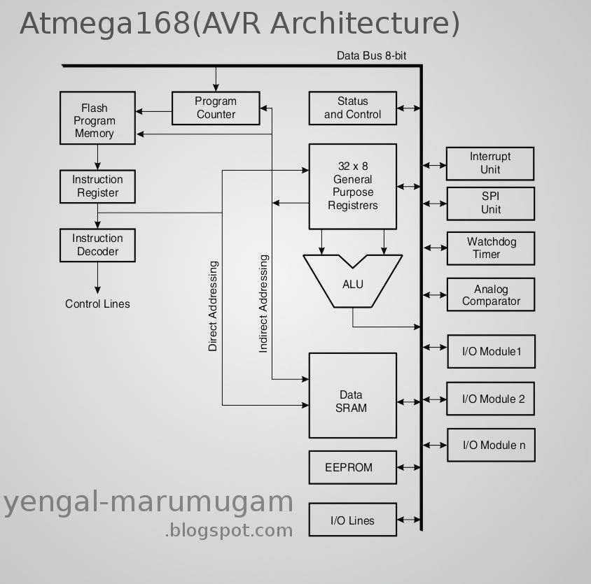
Monday 24 October 2011

SRAM Data memory and Stack Pointer

SRAM data memory:

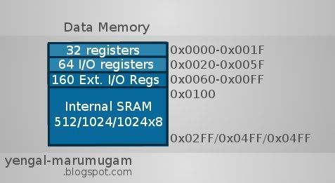
     The data memory is divided into 32 locations for register file, next 64 locations for standard I/O memory, 160 locations for extended I/O memory and the next 1024 (* 1K memory for atmega168) locations for internal data SRAM. (* Internal data memory varies for atmega48/88/168/328 as 512,1K,1K,2K respectively).

   The data memory map of AVR is given in the figure.

Register File:
     A Register file is an array of registers in a CPU. This serves as the central architectural element of any AVR uC. Each register is implemented by using SRAM (static RAM) with dedicated ports for reading and writing. In AVR, the register file is optimized for enhanced RISC (reduced instruction set computing) architecture with single clock cycle access time, which means 2 operands are accessed from 2 registers, the operated is executed and the result is stored in a register in one clock cycle.

Data Transfer between General Purpose Registers and ALU


      The general purpose register file is classified into 32 8-bit registers, namely r0 to r31. Although the register file of AVR is normally perceived as a 32x8 bit storage unit, it is actually a 16x16 unit. This format is necessary for updating 16bit (26 to 31) memory pointers in a single cycle. These memory pointers (ie) 26-27, 28-29, 30-31 pairs serve as 16bit address pointers for indirect addressing of data, named X, Y and Z pointers respectively. These address registers have some special functions like fixed displacement, auto increment and auto decrement. The addressing (00H - 1FH) of each register is given in the following table:


16 x 16 bit array addresses
Address 15-8 (high) 7-0 (low)
00H r1 r0
02H r3 r2
04H r5 r4
06H r7 r6
08H r9 r8
0AH r11 r10
0CH r13 r12
0EH r15 r14
10H r17 r16
12H r19 r18
14H r21 r20
16H r23 r22
18H r25 r24
1AH r27 r26
1CH r29 r28
1EH r31 r30

I/O Memory:
     The CPU consists of several peripherals namely interrupt unit, SPI (Serial Peripheral Interface) unit, control register, Watchdog timer, Analog comparator, I/O modules, etc. The I/O memory contains the addresses of the basic CPU peripheral functions and other I/O functions. The function of each I/O memory location is fixed by the designer. It consists of 64 memory locations called as standard I/O memory. 

Extended I/O Memory:
     Complex microcontrollers like ATmega48/88/68/328 with more ports and peripheral units cannot be supported within the 64 memory locations. Those extra ports and peripherals are supported by the extended I/O memory which contains 160 memory locations( ATmega48/88/68/328 ). The size of extended I/O memory depends on the micro-controller. 

Internal SRAM:
     The Internal SRAM is the general purpose RAM used by the programmer for storing the intermediate values and results. Hence, it is also known as Scratch-pad. They can be accessed directly by using their address and indirectly by pointers (storing their address in register pairs). The memory locations can be accessed sequentially by use of X,Y,Z pointers (which support auto-increment,-decrement). The size of internal SRAM depends on the micro-controller ( discussed in data memory ).

Stack Pointer :
     The Stack is used for storing temporary data, local variables and return addresses after subroutine calls. The stack pointer points to top most memory location of the stack. The stack advances from higher memory location to lower memory location. It is implemented using 2 8-bit registers in I/O space. 


Reference:

  1.  web.alfredstate.edu
  2.  www.atmel.com

Sunday 23 October 2011

CPU Basics

     I was on hunting of resources on fundamentals of CPU. Energy exhausted. Everything  I found was incomplete, irrelevant. Yeah, Internet gives us clues to solve a puzzle. I think I almost solved it.

     Consider any process has to be controlled. Who is to control? CPU is the controlling element of any process. This word appeared for the first time during 1960's in the Industries. In late 1960's microprocessor based CPU's came to rule the industries. The microprocessors require many external components for their operation. This increased the cost of project. So, the manufacturers came up with an idea of integrating the minimal external components inside it, necessary for its operation. As the area of application varies the manufacturer introduced a new device, that has many of the important accessories required by wide range of applications. Its is how our micro-controllers were born.

Microcontroller:
   Micro-controllers = Microprocessor + Memory + Accessories 
The following figure is of Atmega168 architecture.


      CPU is the master of the microcontroller. Every CPU consists of Control Unit(CU) and Arithmetic Logic Unit(ALU).

     Arithmetic Logic Unit: It performs Addition and Logical Operations like ANDing ORing. They when coupled with inverters, it can perform Subtraction, NANDing, NORing etc. You may have studied about the Adder circuits in Digital electronics. They are One bit adders. Four one bit adders combined to form four bit adder, i.e it could add two four bit numbers at a time. Similarly a 32-bit ALU can manipulate 32-bit numbers in one instruction cycle.

    Control Unit: It has several important jobs to perform namely, instruction decoding, memory access, etc.. It activates the components of ALU and other parts of CPU. This is done by passing the specific control code to the components. A most simple Control Unit is a look-up table whose elements are indexed by the opcodes. i.e for every opcode, there is an equivalent control code.

e.g: for the instruction ADD B(add the contents of register 'B' with the contents of Accumulator and stores the results in Accumulator), there will be s series of control codes to activate the adder circuit and pass the operands to the adder, and to activate circuitry to store the result in the Accumulator. 

     Advanced Control Units are designed as Finite State Machines. They work based on the current state they present. It out of scope of this article.

     Other that ALU and CU, CPU consists of Register Bank/File, Status Register, Stack pointer. It is a series of 8-bit registers in 8-bit uC and 16-bit registers in 16-bit uC. These are called general purpose registers. Atmega168 contains 32x8-bit registers. 8085 CPU contains 6x8-bit registers. Status register has 8-bits of information about the previous arithmetic-logic operation.


Bit Symbol Full name Description
0
C
Carry Flag The Carry Flag C indicates a carry in an arithmetic or logic operation.
1
Z
Zero Flag The Zero Flag Z indicates a zero result in an arithmetic or logic operation
2
N
Negative Flag The Negative Flag N indicates a negative result in an arithmetic or logic operation
3
V
Two’s Complement Overflow Flag The Two’s Complement Overflow Flag V supports two’s complement arithmetics
4
S
Sign Bit The S-bit is always an exclusive or between the negative flag N and the two’s complement overflow flag V
5
H
Half Carry Flag The Half Carry Flag H indicates a half carry in some arithmetic operations. Half Carry is
useful in BCD arithmetic
6
T
Bit Copy Storage The Bit Copy instructions BLD (Bit LoaD) and BST (Bit STore) use the T-bit as source or destination for the operated bit. A bit from a register in the Register file can be copied into T by the BST instruction, and a bit in T can be copied into a bit in a register in the Register file by the BLD instruction
7
I
Global Interrupt Enable The Global Interrupt Enable bit must be set for the interrupts to be enabled. The individual interrupt enable control is then performed in separate control registers. If the Global Interrupt Enable Register is cleared, none of the interrupts are enabled independent of the individual interrupt enable settings


8-Bit ALU:
    The figure on the left shows the circuit for one bit operation. It is called One-bit Slice.

    The ALU consists of different section for different operations. These section can be enabled with proper control codes(lines).

    An 8-bit ALU is nothing but the series of ALU Slices cascaded one after another. The figure on the right shows the block diagram representation for the One-bit slice. This is to help the interpretation of following 8-Bit ALU.


Coming Up Next:

* AVR Instruction Set

Basics of Burning

     Making a micro-controller to work is not a simple one. It consists of different processes, namely coding, compiling, burning(device programming), on the software side. On the hardware side it consists of providing a clock, proper supply voltage(refer datasheet). These are the compulsory requirements for a micro-controller to work.

       Coding and compiling can be easily understood, because there are many tutorials in the internet. Burning and last important step for operation of micro-controller. Burning is the process of writing the compiled program(hex data) into the program memory of micro-controller. 

      To understand how burning works it is necessary to understand the CPU basics.  Here is a simplified explanation for it.

     CPU is a logical circuitry that executes the instructions from the RAM. The program can be stored in any permanent (memory) storage device. The program can be loaded into RAM from the permanent memory, then the CPU interprets the instructions from the RAM and executes it.

     CPU can store the contents (the program) from the RAM in any other storage devices, the program storage device too. Here afterwards we call program storage will simply called program memory.

    From the above description,we are clear that, it is enough for us to load the program into the RAM. The micro-controllers have instruction to to feed the RAM with the input from serial or parallel ports. This how it is going to store the program from our computer into program memory.

(to be continued)

Saturday 22 October 2011

Monostable Multivibrator- Debouncing

What is de-bouncing?

Consider a simple push button connected to 5V supply. When the push button is pressed and released the signal across the output terminal of the button and the ground is expected to be like a signal given below:


But the actual signal looks like this:


As we can see from the above figure, bouncing of signal occurs during the transient time when mechanical switches are used, due to their surface roughness. This bouncing of wave should be avoided for proper functioning of the circuit in which the switch is used. This is known as switch de-bouncing. 

How is it done?

As mentioned in the previous post Monostable Multivibrator- 555 timer, a monostable multivibrator (MSMV) can be used for debouncing. We here by,  use 555 timer for that purpose.


Components Required:

1. IC 555
2. Resistor 10Kohm
3. Capacitors 10uF, 0.01uF
4. 5V supply

Design:

We need to design the timing resistors and capacitor values depending on the need. The time for which the MSMV remains in unstable state is given by the equation:
T=1.0986*R*C

For R=10Kohm and C=10uF, we get a time delay of approximately 110ms. 

Circuit Diagram:

A Simple Application:

Let us now use the 555 timer in MSMV mode in the following test circuit. 

About the test circuit:

In the above circuit we use IC4029 to count the number of times the SPDT switch SW1 is pulled to ground(0V) and 5V. The number of counts is displayed in binary form using 4 LED's which count up-to 15 and then resets. Since the switch used is a mechanical device, waveform bouncing occurs which is rectified by the 555timer in MSMV mode. The wire from the output terminal of switch is connected to the trigger(pin2) of the 555timer and the output(pin3) is connected to the clock(pin15) of the counter.

A time delay of 110ms is obtained by placing suitable timing resistor and capacitor. 


Sample Input and Output Waveforms:


Reference:

Friday 21 October 2011

Digital Voltmeter - Part II

Ramp Type DVM
  

The block diagram of the Ramp type ADC is given below. The principle and working of the Ramp type ADC is explained in a simplified manner in this post.
The merits and demerits of the Ramp type ADC is also listed at the end of the post.


Block Diagram:


Principle: 

Input voltage is converted into digital equivalent by counting the time taken for the ramp wave to decrease from the magnitude of input voltage to 0V.

Construction:

The block diagram of the Ramp-type ADC can be divided into two sections as follows:
      1. Voltage to time conversion section
      2. Time measurement section

In the voltage to time conversion section, the analog input voltage is fed to the attenuation circuit. The attenuated signal is compared with the the ramp signal generated by the ramp generator given in the block diagram by the input comparator 'C1'. Similarly, The ramp signal generated is compared with 0V via a zero-crossing detector 'C2'. A sample rate multivibrator is connected to the ramp generator whose purpose is to provide an initiating pulse for the ramp generator to start the next ramp voltage for the next measurement. It is also used to reset the counter before generating the next ramp voltage.

In the time measurement section, there is counter which is triggered by a gating pulse. The inputs of the gating pulse are (i) Output of 'C1' (ii) Output of 'C2' (iii) Clock pulse from the oscillator. The counter is reset after each successful completion of time measurement by a control signal from the sample rate multivibrator. The count produced is displayed by connecting suitable display device.


Detailed Operation:

Initially, the attenuated signal is compared with a negative going ramp signal generated by the ramp generator. When the ramp voltage coincides with the input signal, the output of 'C1' becomes low. This point is called coincidence point. This initiates the counting process ( start of count ). The counter continues to count until the ramp voltage reduces and crosses zero (0V). This is detected by zero crossing detector 'C2'. The output of 'C2' becomes high which ends the counting process (end of count).


The count displayed is the count of number of clock pulses produced by the oscillator during the time in which the ramp signal is less than the input signal and greater than 0V (ie)  |input signal| > ramp > 0V. This count gives the digital equivalent of input analog voltage.

Equations Involved:

(del)t = t2 - t1= Vin/m = nT ;
 Hence, Vin = nmT;

where
 t1-> start of count
 t2-> end of count
 Vin-> input analog voltage
 m-> slope of the ramp curve
 n-> number of clock pulses to counter
 T-> clock period


Merits:
* low cost
* simple, easy to design
* long distance transmission of output pulse is possible


Demerits:
* accuracy of output greatly depends on linearity of the ramp.
   (since only one ramp is used)
* input filter are needed for filtering noise from input signal.


References:
1. microscope-multimeter.info
2. pioneer.netserv.chula.ac.th
3. indiastudychannel.com
4. en.wikipedia.org


Coming up next:

* Integrating Type DVM
* Successive Approximation type DVM


Share

Twitter Delicious Facebook Digg Stumbleupon Favorites More