SRAM data memory:
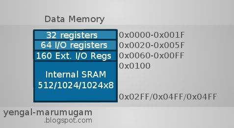
 The data memory is divided into 32 locations for register file, next 64 locations for standard I/O memory, 160 locations for extended I/O memory and the next 1024 (* 1K memory for atmega168) locations for internal data SRAM. (* Internal data memory varies for atmega48/88/168/328 as 512,1K,1K,2K respectively).
The data memory map of AVR is given in the figure.
Register File:
A Register file is an array of registers in a CPU. This serves as the central architectural element of any AVR uC. Each register is implemented by using SRAM (static RAM) with dedicated ports for reading and writing. In AVR, the register file is optimized for enhanced RISC (reduced instruction set computing) architecture with single clock cycle access time, which means 2 operands are accessed from 2 registers, the operated is executed and the result is stored in a register in one clock cycle.
The general purpose register file is classified into 32 8-bit registers, namely r0 to r31. Although the register file of AVR is normally perceived as a 32x8 bit storage unit, it is actually a 16x16 unit. This format is necessary for updating 16bit (26 to 31) memory pointers in a single cycle. These memory pointers (ie) 26-27, 28-29, 30-31 pairs serve as 16bit address pointers for indirect addressing of data, named X, Y and Z pointers respectively. These address registers have some special functions like fixed displacement, auto increment and auto decrement. The addressing (00H - 1FH) of each register is given in the following table:
 The data memory is divided into 32 locations for register file, next 64 locations for standard I/O memory, 160 locations for extended I/O memory and the next 1024 (* 1K memory for atmega168) locations for internal data SRAM. (* Internal data memory varies for atmega48/88/168/328 as 512,1K,1K,2K respectively).
The data memory map of AVR is given in the figure.
Register File:
A Register file is an array of registers in a CPU. This serves as the central architectural element of any AVR uC. Each register is implemented by using SRAM (static RAM) with dedicated ports for reading and writing. In AVR, the register file is optimized for enhanced RISC (reduced instruction set computing) architecture with single clock cycle access time, which means 2 operands are accessed from 2 registers, the operated is executed and the result is stored in a register in one clock cycle.
Data Transfer between General Purpose Registers and ALU
| Address | 15-8 (high) | 7-0 (low) |
|---|---|---|
| 00H | r1 | r0 |
| 02H | r3 | r2 |
| 04H | r5 | r4 |
| 06H | r7 | r6 |
| 08H | r9 | r8 |
| 0AH | r11 | r10 |
| 0CH | r13 | r12 |
| 0EH | r15 | r14 |
| 10H | r17 | r16 |
| 12H | r19 | r18 |
| 14H | r21 | r20 |
| 16H | r23 | r22 |
| 18H | r25 | r24 |
| 1AH | r27 | r26 |
| 1CH | r29 | r28 |
| 1EH | r31 | r30 |
Reference:


.JPG)


0 comments:
Post a Comment
தங்களது கருத்துக்களை இங்கே வெளியிடவும்...