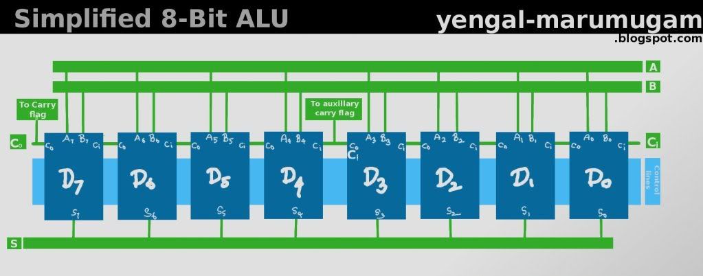
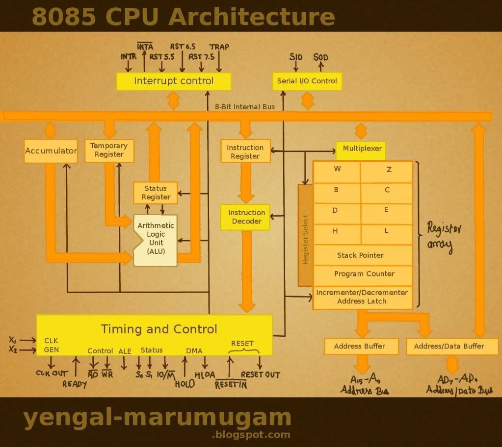
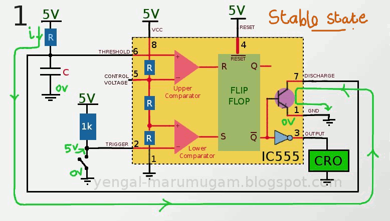
Sunday 4 December 2011

Interfacing PS2 Controller with Arduino

    In the previous post PS2 Controller Outline, the pin configuration, specifications and working of different buttons of PS2 controller are explained. In this post we interface the controller with an Arduino development board and test a sample program. We seperate this into two sections; the hardware and software sections. The hardware section is pretty much straight forward which involves connecting controller wires to arduino pins. In the software section, we use the PS2X class in "PS2 controller Arduino Library v1.4" provided by billporter.

Hardware Section:

    Out of 9 wires from the PS2 controller, we here use only 6 pins. They are Vcc(red), gnd(black), clock(blue), command(orange), attention(yellow), data(brown).


PS2 Controller Pins Arduino Pins
Vcc 3V3 pin of on-board FTDI chip
gnd digital ground pin
*clock pin 13
*command pin 11
*attention pin 10
**data pin 12


    * Note1: clk, cmd, att, data can be connected to any of the digital pins and program can be modified accordingly.

  ** Note2: The data pin should be connected as shown in the figure

Software Section: 
    The library is available for download at billporter. In the PS2X class, all the button states are defined as constants as given below:


Some of the important functions defined are given below:

1. config_gamepad(clock,command,attention,data,Pressures?,Rumble?)
                 This function configures the PS2 controller and returns a corresponding result in byte format. The pins to which clk, cmd, att and data are connected should be entered in this function for initial setup. Pressure and Rumble are boolean values which can be enabled or disabled.

2. read_gamepad()
                This function is called to get new values from the controller. This should be called atleast once in a second. It can also be used to set vibration strength of the vibrating motor.

3. Button(Button_Constant)
                This function returns a boolean value depending on whether a button is pressed or not. It takes a button constant as argument.

4. Analog(Button_Constant)
                This function takes Button_Constant as argument and returns a byte which represents the analog value of the button (ie) the position in case of stick and the pressure with which the button is pressed in case of pressure button.

5. ButtonPressed(Button_Constant)
                It returns a boolean value based on whether a button is just pressed or not.

6. ButtonReleased(Button_Constant)
               It returns a boolean value based on whether a button is just released or not.


7. NewButtonState(Button_constant)
                             It returns a boolean value based on change in button state.


Sample Code:
    Having discussed the software and hardware sections, lets now examine the example code given in the library itself. Click here to view the sketch "PS2X_Example".


ALGORITHM:
  • Include PS2X_lib.h
  • Create an instance for PS2X class

SETUP:

  • Set baud rate
  • Configure the game pad
  • Identify the controller type 
  • Display results in Serial Monitor

LOOP:

  • Read game pad ( read_gamepad( ) )
  • Check all the button states 
  • If any button is pressed, display it in serial monitor
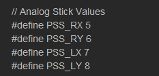
  • If L1 or R1 is pressed, display the analog stick values in serial monitor
  • Call a delay of 50 milliseconds.
Screenshot of serial monitor:


Monday 24 October 2011

SRAM Data memory and Stack Pointer

SRAM data memory:

     The data memory is divided into 32 locations for register file, next 64 locations for standard I/O memory, 160 locations for extended I/O memory and the next 1024 (* 1K memory for atmega168) locations for internal data SRAM. (* Internal data memory varies for atmega48/88/168/328 as 512,1K,1K,2K respectively).

   The data memory map of AVR is given in the figure.

Register File:
     A Register file is an array of registers in a CPU. This serves as the central architectural element of any AVR uC. Each register is implemented by using SRAM (static RAM) with dedicated ports for reading and writing. In AVR, the register file is optimized for enhanced RISC (reduced instruction set computing) architecture with single clock cycle access time, which means 2 operands are accessed from 2 registers, the operated is executed and the result is stored in a register in one clock cycle.

Data Transfer between General Purpose Registers and ALU


      The general purpose register file is classified into 32 8-bit registers, namely r0 to r31. Although the register file of AVR is normally perceived as a 32x8 bit storage unit, it is actually a 16x16 unit. This format is necessary for updating 16bit (26 to 31) memory pointers in a single cycle. These memory pointers (ie) 26-27, 28-29, 30-31 pairs serve as 16bit address pointers for indirect addressing of data, named X, Y and Z pointers respectively. These address registers have some special functions like fixed displacement, auto increment and auto decrement. The addressing (00H - 1FH) of each register is given in the following table:


16 x 16 bit array addresses
Address 15-8 (high) 7-0 (low)
00H r1 r0
02H r3 r2
04H r5 r4
06H r7 r6
08H r9 r8
0AH r11 r10
0CH r13 r12
0EH r15 r14
10H r17 r16
12H r19 r18
14H r21 r20
16H r23 r22
18H r25 r24
1AH r27 r26
1CH r29 r28
1EH r31 r30

I/O Memory:
     The CPU consists of several peripherals namely interrupt unit, SPI (Serial Peripheral Interface) unit, control register, Watchdog timer, Analog comparator, I/O modules, etc. The I/O memory contains the addresses of the basic CPU peripheral functions and other I/O functions. The function of each I/O memory location is fixed by the designer. It consists of 64 memory locations called as standard I/O memory. 

Extended I/O Memory:
     Complex microcontrollers like ATmega48/88/68/328 with more ports and peripheral units cannot be supported within the 64 memory locations. Those extra ports and peripherals are supported by the extended I/O memory which contains 160 memory locations( ATmega48/88/68/328 ). The size of extended I/O memory depends on the micro-controller. 

Internal SRAM:
     The Internal SRAM is the general purpose RAM used by the programmer for storing the intermediate values and results. Hence, it is also known as Scratch-pad. They can be accessed directly by using their address and indirectly by pointers (storing their address in register pairs). The memory locations can be accessed sequentially by use of X,Y,Z pointers (which support auto-increment,-decrement). The size of internal SRAM depends on the micro-controller ( discussed in data memory ).

Stack Pointer :
     The Stack is used for storing temporary data, local variables and return addresses after subroutine calls. The stack pointer points to top most memory location of the stack. The stack advances from higher memory location to lower memory location. It is implemented using 2 8-bit registers in I/O space. 


Reference:

  1.  web.alfredstate.edu
  2.  www.atmel.com

Sunday 23 October 2011

CPU Basics

     I was on hunting of resources on fundamentals of CPU. Energy exhausted. Everything  I found was incomplete, irrelevant. Yeah, Internet gives us clues to solve a puzzle. I think I almost solved it.

     Consider any process has to be controlled. Who is to control? CPU is the controlling element of any process. This word appeared for the first time during 1960's in the Industries. In late 1960's microprocessor based CPU's came to rule the industries. The microprocessors require many external components for their operation. This increased the cost of project. So, the manufacturers came up with an idea of integrating the minimal external components inside it, necessary for its operation. As the area of application varies the manufacturer introduced a new device, that has many of the important accessories required by wide range of applications. Its is how our micro-controllers were born.

Microcontroller:
   Micro-controllers = Microprocessor + Memory + Accessories 
The following figure is of Atmega168 architecture.


      CPU is the master of the microcontroller. Every CPU consists of Control Unit(CU) and Arithmetic Logic Unit(ALU).

     Arithmetic Logic Unit: It performs Addition and Logical Operations like ANDing ORing. They when coupled with inverters, it can perform Subtraction, NANDing, NORing etc. You may have studied about the Adder circuits in Digital electronics. They are One bit adders. Four one bit adders combined to form four bit adder, i.e it could add two four bit numbers at a time. Similarly a 32-bit ALU can manipulate 32-bit numbers in one instruction cycle.

    Control Unit: It has several important jobs to perform namely, instruction decoding, memory access, etc.. It activates the components of ALU and other parts of CPU. This is done by passing the specific control code to the components. A most simple Control Unit is a look-up table whose elements are indexed by the opcodes. i.e for every opcode, there is an equivalent control code.

e.g: for the instruction ADD B(add the contents of register 'B' with the contents of Accumulator and stores the results in Accumulator), there will be s series of control codes to activate the adder circuit and pass the operands to the adder, and to activate circuitry to store the result in the Accumulator. 

     Advanced Control Units are designed as Finite State Machines. They work based on the current state they present. It out of scope of this article.

     Other that ALU and CU, CPU consists of Register Bank/File, Status Register, Stack pointer. It is a series of 8-bit registers in 8-bit uC and 16-bit registers in 16-bit uC. These are called general purpose registers. Atmega168 contains 32x8-bit registers. 8085 CPU contains 6x8-bit registers. Status register has 8-bits of information about the previous arithmetic-logic operation.


Bit Symbol Full name Description
0
C
Carry Flag The Carry Flag C indicates a carry in an arithmetic or logic operation.
1
Z
Zero Flag The Zero Flag Z indicates a zero result in an arithmetic or logic operation
2
N
Negative Flag The Negative Flag N indicates a negative result in an arithmetic or logic operation
3
V
Two’s Complement Overflow Flag The Two’s Complement Overflow Flag V supports two’s complement arithmetics
4
S
Sign Bit The S-bit is always an exclusive or between the negative flag N and the two’s complement overflow flag V
5
H
Half Carry Flag The Half Carry Flag H indicates a half carry in some arithmetic operations. Half Carry is
useful in BCD arithmetic
6
T
Bit Copy Storage The Bit Copy instructions BLD (Bit LoaD) and BST (Bit STore) use the T-bit as source or destination for the operated bit. A bit from a register in the Register file can be copied into T by the BST instruction, and a bit in T can be copied into a bit in a register in the Register file by the BLD instruction
7
I
Global Interrupt Enable The Global Interrupt Enable bit must be set for the interrupts to be enabled. The individual interrupt enable control is then performed in separate control registers. If the Global Interrupt Enable Register is cleared, none of the interrupts are enabled independent of the individual interrupt enable settings


8-Bit ALU:
    The figure on the left shows the circuit for one bit operation. It is called One-bit Slice.

    The ALU consists of different section for different operations. These section can be enabled with proper control codes(lines).

    An 8-bit ALU is nothing but the series of ALU Slices cascaded one after another. The figure on the right shows the block diagram representation for the One-bit slice. This is to help the interpretation of following 8-Bit ALU.


Coming Up Next:

* AVR Instruction Set

Basics of Burning

     Making a micro-controller to work is not a simple one. It consists of different processes, namely coding, compiling, burning(device programming), on the software side. On the hardware side it consists of providing a clock, proper supply voltage(refer datasheet). These are the compulsory requirements for a micro-controller to work.

       Coding and compiling can be easily understood, because there are many tutorials in the internet. Burning and last important step for operation of micro-controller. Burning is the process of writing the compiled program(hex data) into the program memory of micro-controller. 

      To understand how burning works it is necessary to understand the CPU basics.  Here is a simplified explanation for it.

     CPU is a logical circuitry that executes the instructions from the RAM. The program can be stored in any permanent (memory) storage device. The program can be loaded into RAM from the permanent memory, then the CPU interprets the instructions from the RAM and executes it.

     CPU can store the contents (the program) from the RAM in any other storage devices, the program storage device too. Here afterwards we call program storage will simply called program memory.

    From the above description,we are clear that, it is enough for us to load the program into the RAM. The micro-controllers have instruction to to feed the RAM with the input from serial or parallel ports. This how it is going to store the program from our computer into program memory.

(to be continued)

Saturday 22 October 2011

Monostable Multivibrator- Debouncing

What is de-bouncing?

Consider a simple push button connected to 5V supply. When the push button is pressed and released the signal across the output terminal of the button and the ground is expected to be like a signal given below:


But the actual signal looks like this:


As we can see from the above figure, bouncing of signal occurs during the transient time when mechanical switches are used, due to their surface roughness. This bouncing of wave should be avoided for proper functioning of the circuit in which the switch is used. This is known as switch de-bouncing. 

How is it done?

As mentioned in the previous post Monostable Multivibrator- 555 timer, a monostable multivibrator (MSMV) can be used for debouncing. We here by,  use 555 timer for that purpose.


Components Required:

1. IC 555
2. Resistor 10Kohm
3. Capacitors 10uF, 0.01uF
4. 5V supply

Design:

We need to design the timing resistors and capacitor values depending on the need. The time for which the MSMV remains in unstable state is given by the equation:
T=1.0986*R*C

For R=10Kohm and C=10uF, we get a time delay of approximately 110ms. 

Circuit Diagram:

A Simple Application:

Let us now use the 555 timer in MSMV mode in the following test circuit. 

About the test circuit:

In the above circuit we use IC4029 to count the number of times the SPDT switch SW1 is pulled to ground(0V) and 5V. The number of counts is displayed in binary form using 4 LED's which count up-to 15 and then resets. Since the switch used is a mechanical device, waveform bouncing occurs which is rectified by the 555timer in MSMV mode. The wire from the output terminal of switch is connected to the trigger(pin2) of the 555timer and the output(pin3) is connected to the clock(pin15) of the counter.

A time delay of 110ms is obtained by placing suitable timing resistor and capacitor. 


Sample Input and Output Waveforms:


Reference:

Friday 21 October 2011

Digital Voltmeter - Part II

Ramp Type DVM
  

The block diagram of the Ramp type ADC is given below. The principle and working of the Ramp type ADC is explained in a simplified manner in this post.
The merits and demerits of the Ramp type ADC is also listed at the end of the post.


Block Diagram:


Principle: 

Input voltage is converted into digital equivalent by counting the time taken for the ramp wave to decrease from the magnitude of input voltage to 0V.

Construction:

The block diagram of the Ramp-type ADC can be divided into two sections as follows:
      1. Voltage to time conversion section
      2. Time measurement section

In the voltage to time conversion section, the analog input voltage is fed to the attenuation circuit. The attenuated signal is compared with the the ramp signal generated by the ramp generator given in the block diagram by the input comparator 'C1'. Similarly, The ramp signal generated is compared with 0V via a zero-crossing detector 'C2'. A sample rate multivibrator is connected to the ramp generator whose purpose is to provide an initiating pulse for the ramp generator to start the next ramp voltage for the next measurement. It is also used to reset the counter before generating the next ramp voltage.

In the time measurement section, there is counter which is triggered by a gating pulse. The inputs of the gating pulse are (i) Output of 'C1' (ii) Output of 'C2' (iii) Clock pulse from the oscillator. The counter is reset after each successful completion of time measurement by a control signal from the sample rate multivibrator. The count produced is displayed by connecting suitable display device.


Detailed Operation:

Initially, the attenuated signal is compared with a negative going ramp signal generated by the ramp generator. When the ramp voltage coincides with the input signal, the output of 'C1' becomes low. This point is called coincidence point. This initiates the counting process ( start of count ). The counter continues to count until the ramp voltage reduces and crosses zero (0V). This is detected by zero crossing detector 'C2'. The output of 'C2' becomes high which ends the counting process (end of count).


The count displayed is the count of number of clock pulses produced by the oscillator during the time in which the ramp signal is less than the input signal and greater than 0V (ie)  |input signal| > ramp > 0V. This count gives the digital equivalent of input analog voltage.

Equations Involved:

(del)t = t2 - t1= Vin/m = nT ;
 Hence, Vin = nmT;

where
 t1-> start of count
 t2-> end of count
 Vin-> input analog voltage
 m-> slope of the ramp curve
 n-> number of clock pulses to counter
 T-> clock period


Merits:
* low cost
* simple, easy to design
* long distance transmission of output pulse is possible


Demerits:
* accuracy of output greatly depends on linearity of the ramp.
   (since only one ramp is used)
* input filter are needed for filtering noise from input signal.


References:
1. microscope-multimeter.info
2. pioneer.netserv.chula.ac.th
3. indiastudychannel.com
4. en.wikipedia.org


Coming up next:

* Integrating Type DVM
* Successive Approximation type DVM


Wednesday 21 September 2011

PS2 Controller - Simple Outline


The PlayStation brand is a series of video game consoles created and developed by Sony Computer Entertainment. In this post we concentrate on how the (playstation 2) PS2 controller functions. The PS2 controller consists of 4 main select buttons ‘Triangle’, ‘Circle’, ‘Cross’ and square, start, select, a D-pad, shoulder buttons ( L1, L2, R1, R2 ) and 2 analog sticks with Dual shock feature. All the buttons are pressure-sensitive except start and select.


How is pressure-sensitivity achieved?


Whenever a button is pressed, a small disc attached to the bottom of the button is pushed against the conductive strip mounted on the circuit board of the controller. With increase in pressure applied over the button, area of the disc touching the strip is increased and so there is an increase in conductivity leading to increase in flow of current. Thus, the buttons are made pressure-sensitive.


What is dual shock feature? How is it achieved?

         The Dual Shock feature provides a tactile stimulation to certain actions in a game. It makes us feel the vibration during the some critical situations in the game. It is achieved by means of 2 dc vibration motors ( left and right ).


        To the shaft of each motor, an unbalanced weight is attached. When the motor rotates, due to imbalance of weight, it wobbles which is experienced as vibration by the user.


How do analog sticks work?
        Beneath the analog stick, 2 potentiometers (bc103, 10K) are mounted at right angles to each other, one for vertical and the other for horizontal movements. 


          Whenever the joystick is moved in horizontal or vertical direction, there is a corresponding change in the resistance of corresponding POT. Due to this variation in resistance, there is a change in current flowing through it.

Schematic:


Pin Out:


Pin Name Description
1 DATA Data
2 CMD Command
3 +7.6V Dualshock and Dualshock 2 uses this for powering vibro-motors. Voltage on PS2 is 7.6V(standard)/9V
4 GND Ground
5 VCC Vcc
6 ATT ATT select
7 CLK Clock
8 N/C No connection
9 ACK Acknowledge


Pin Details:

  • Data:  This signal is an 8 bit serial transmission synchronous to the falling edge of clock
  • Command: This signal is the counter part of DATA. It is again an 8 bit serial transmission on the falling edge of clock.
  • ATT(Select/DTR/Command): ATT is used to get the attention of the controller.This signal will go low for the duration of a transmission.
  • Clock: (from PSX to Controller) Used to keep units in sync.
  • ACK (from Controller to PSX): This signal should go low for at least one clock period after each 8 bits are sent and ATT is still held low.


More Info on PlayStation:


Coming up next:

Tuesday 20 September 2011

Monostable Multivibrator- 555 timer

             It is a electronic circuitry (more specifically a relaxation oscillator), that maintains a HIGH or LOW at the output terminal for a fixed period of time interval (determined by  resistor capacitor pair), when a trigger is being given at the input. Other name is One-shot multivibrator.

       What the name indicates, is that the output has only one stable state. When triggered it goes to unstable state, remains there for some time and get back to stable state.

        We'll construct the circuit first with OpAmp and then with 555-timer IC.

555 TIMER:
        The following circuit is the monostable multivibrator using 555-TIMER (IC NE555N). Briefly, the charging time of the circuit determines the time period of the output waveform.

555 Timer Block diagram and its Monostable Multivibrator Configuration.
     555 timer IC consists of a RS flip-flop whose Set and Reset terminals controlled by two comparators, and a three resistor potential divider network, which divides the supply voltage into three equal voltages . In case the supply voltage is 5V, it divided in three resistors as 1.667V. Therefore, the inverting terminal of the upper comparator is connected to 2Vcc/3 = 3.334V and the non-inverting terminal of lower comparator is connected to Vcc/3 = 1.667V. In addition 555 Timer IC also contains a NPN transistor. Its emitter terminal is grounded and collector terminal is called 'Discharge' to which we can connect external potential point that can be drained with the help of transistor. The transistor is operated by the RS flip-flop, since its base terminal is connected to the Q' terminal of RS flip-flop.

Monostable Multivibrator Operation:
     The circuit remains in stable state(LOGICAL-LOW for this circuit), as the current from the supply for RC pair is not allowed to charge the capacitor. At the time of start the, since the FLIPFLOP is reset, the Q' is HIGH(+5V). This drives the transistor into ON condition(saturation region). The functioning of the transistor is clearly understandable from the following figure:
     
   
How the Monostable multivibrator is driven into unstable state? 
  When the trigger is applied(i.e switch is closed), the 'Trigger' terminal (inerting terminal of lower comparator)  is directly connected to the ground(0V). This toggles the output of lower comparator from LOW to HIGH. So the SET terminal of FLIPFLOP is at HIGH, toggling the Q' to LOW. The output is HIGH.


How the Monostable multivibrator recovers from unstable state?
     As we have seen above the Q' is toggled from HIGH to LOW, which inturn turns-OFF the transistor. The capacitor(C) charges through Resistor(R). When the capacitor voltages just rises above the voltage at the inverting terminal of upper comparator, it toggles its output from LOW to HIGH. This resets the FLIPFLOP, i.e the Q' is again set to HIGH. Thus the transistor is driven into saturation and the cycle continues.

    When the trigger is given, the output is toggles for a finite time period determined by the time constant = RC.

The design formula derivation is shown below. The capacitor charging equation is used to derive the expression for On-time(unstable-state) for the output waveform. Vf is the voltage of the capacitor, if it is allowed to charge for infinite time period. It is equal to the given supply voltage. The figures on the right and below explain the derivation more elaborately.

   The main application of Monostable multivibrator is switch debouncing, where multiple pulses are generated for single press of the switch. It is also used for the conversion of frequency into proportional voltage. In my next post we will learn about the frequency to voltage(F/V) conversion.


Coming up next:
* Frequency to Voltage Conversion
* Application: Switch Debouncing


Tuesday 16 August 2011

8255 Programmable Peripheral Interface


         In this post, we are going to learn a very old grand father of modern processors, named 8085 and his colleague 8255.

Pins, Signals and internal block diagram of 8255: 


  •  The internal block diagram of 8255 is shown in fig: 
  •  The 8255 can be either memory mapped or I/O mapped in the system. In the schematic shown in above is I/O mapped in the system. 
  •  Using a 3-to-8 decoder generates the chip select signals for I/O mapped devices. 
  • The address lines A4, A5 and A6 are decoded to generate eight chip select signals (IOCS-0 to IOCS-7) and in this, the chip select IOCS- 1 is used to select 8255. 
  • The address line A7 and the control signal IO/M (low) are used as enable for the decoder. 
  • The address line A0 of 8085 is connected to A0 of 8255 and A1 of 8085 is connected to A1 of 8255 to provide the internal addresses. 
  • The data lines D0-D7 are connected to D0-D7 of the processor to achieve parallel data transfer. 
  •  The I/O addresses allotted to the internal devices of 8255 are listed in table. 
              It has 40 pins and requires a single +5V supply.  The INTEL 8255 is a device used to parallel data transfer between processor and slow peripheral devices like ADC, DAC, keyboard, 7-segment display, LCD, etc.  


               The 8255 has three ports: Port-A, Port-B and Port-C.  Port-A can be programmed to work in any one of the three operating modes mode-0, mode-1 and mode-2 as input or output port.  Port-B can be programmed to work either in mode-0 or mode-1 as input or output port. 
               
               Port-C (8-pins) has different assignments depending on the mode of port-A and port-B. If port-A and B are programmed in mode-0, then the port-C can perform any one of the following functions. As 8-bit parallel port in mode-0 for input or output. As two numbers of 4-bit parallel ports in mode-0 for input or output. The individual pins of port-C can be set or reset for various control applications. 


               If port-A is programmed in mode- 1/mode-2 and port-B is programmed in mode-1 then some of the pins of port-C are used for handshake signals and the remaining pins can be used as input/ output lines or individually set/reset for control applications.  The read/write control logic requires six control signals. These signals are given below:

  1. RD (low): This control signal enables the read operation. When this signal is low, the microprocessor reads data from a selected I/O port of the 8255A. 
  2. WR (low): This control signal enables the write operation. When this signal goes low, the microprocessor writes into a selected I/O port or the control register. 
  3. RESET: This is an active high signal. It clears the control register and set all ports in the input mode. 
  4. CS (low), A0 and A1:  These are device select signals. They are, Interfacing of 8255 with 8085 processor:     


Friday 29 July 2011

8085 Instruction set - Branch Instructions

             The branching instructions alter the normal sequential program either conditionaly or unconditionally.


As formerly seen in my previous posts in this Series, we divided the Series into four parts:

UNCONDITIONAL BRANCHING INSRTRUCTIONS:

     JMP :
          This instruction is used to jump from one set of programs to another set
                e.g:   In a 8 bit multiplication program, JN2 LOOP it means that if no zero results in previous arithmetic operation, it will jump to LOOP.
    CALL :
          This instruction is used to call the function.
                e.g:   CALL DIV,CALL SUB etc..
    RET :
          This instruction is used to return to the program after doing some manipulation for a program to succeed.

CONDITIONAL BRANCHING INSTRUCTIONS :
          Here we are going to discuss some instructions which we use with jump instruction.
The instructions are

        NZ Not Zero (Z = 0)
        Z    Zero (Z = 1)
        NC No Carry (C = 0)
        C    Carry (C = 1)
        PO Parity Odd (P = 0)
        PE Parity Even (P = 1)
        P   Plus (S = 0)
        M  Minus (S = 1)

        Jumps Calls Returns
        C CC RC (Carry)
        INC CNC RNC (No Carry)
        JZ CZ RZ (Zero)
        JNZ CNZ RNZ (Not Zero)
        JP CP RP (Plus)
        JM CM RM (Minus)
        JPE CPE RPE (Parity Even)
        JP0 CPO RPO (Parity Odd)
        
        Two other instructions can affect a branch by replacing the contents or the program counter:

        PCHL Move H & L to Program Counter
        RST    Special Restart Instruction Used with Interrupts

Stack I/O, and Machine Control Instructions:
    The following instructions affect the Stack and/or Stack Pointer:

        PUSH  Push Two bytes of Data onto the Stack
        POP     Pop Two Bytes of Data off the Stack
        XTHL Exchange Top of Stack with H & L
        SPHL  Move content of H & L to Stack Pointer

The I/0 instructions are as follows:
        IN     Initiate Input Operation
        OUT Initiate Output Operation

The Machine Control instructions are as follows:
        EI      Enable Interrupt System
        DI     Disable Interrupt System
        HLT Halt
        NOP No Operation

Share

Twitter Delicious Facebook Digg Stumbleupon Favorites More